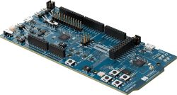
NRF5340-DK


Abbildung kann vom Original abweichen
Download the free Library Loader to convert this file for your ECAD Tool
- Frequenz min
- 2408 MHz
- Frequenz max
- 2480 MHz
- Datenübertragung
- 2000 kbps
- Betriebs Temperatur min.
- -40 °C
- Datenspeicher
- FLASH
- Datenspeichergröße
- 1280 kB
- MCU Architektur
- 32 bit
- Versorgungsspannung max.
- 1.7 V
- P(out)
- 8 dBm
- Empfindlichkeit
- -104 dBm
- RAM
- 320 kB
- ADC Auflösung max
- 12 bit
- ADC Kanäle
- 10 no.
- SPI
- YES
- USB
- YES
- I²C
- YES
- andere Schnittstelle
- UART QSPI
- IEEE802.15.4
- YES
- IEEE802.15.1
- NO
- Betriebs Temperatur max.
- 105 °C
- Versorgungsspannung max.
- 5.5 V
- Automotive
- NO
- RoHS Status
- RoHS-conform
- Verpackung
- INDIVIDUAL
- ECCN
- EAR99
- Zolltarifnummer
- 85437090990
- Land
- Norway
- ABC-Schlüssel
- A
- Lieferzeit beim Hersteller
- 16 Wochen
Development kit for the nRF5340, a dual processor SoC supporting Bluetooth 5.2, Bluetooth mesh, NFC, Thread, and Zigbee
The nRF5340 DK is the development kit for the nRF5340 System-on-Chip (SoC), containing everything needed to get started with development, on a single board.
The DK supports development with an extensive range of wireless protocols. It supports Bluetooth Low Energy with features such as high-throughput 2 Mbps, Advertising Extensions and Long Range. Mesh protocols like Bluetooth mesh, Thread and Zigbee can run concurrently with Bluetooth LE, enabling smartphones to provision, commission, configure and control mesh nodes. NFC, ANT, 802.15.4 and 2.4 GHz proprietary protocols are also supported.
All analog and digital interfaces, and GPIOs are available via headers and edge connectors. The kit is Arduino Uno Rev3 hardware compatible, meaning it can be easily interfaced with external device shields.
Four buttons and four LEDs simplify input and output to and from the nRF5340 SoC, and are all user-programmable. An on-board external memory is connected to the 96 MHz QSPI peripheral in the nRF5340 SoC.
The DK is bundled with an NFC antenna that quickly enables testing of nRF5340’s NFC-A tag functionality. A SEGGER J-Link debugger is on the board, enabling full-blown programming and debugging, of both the nRF5340 SoC and external targets.
The nRF5340 DK is typically powered via USB, but can be powered by a wide range of sources, within the supply range of 1.7 to 5.0 V. In addition to USB, it can be powered with external source, but it also includes a CR2032 battery holder and a Li-Po battery connector, for in-field testing. Current consumption can be measured by using the dedicated current measurement pins, for example by using Nordic’s Power Profiler Kit II.
Die Artikel im Warenkorb können Sie verbindlich bestellen, oder - falls Sie weitere Fragen haben - als unverbindliche Anfrage an uns schicken.
Der Rutronik24 Shop ist nur für Firmenkunden. Ein Verkauf an Privatkunden ist nicht möglich.


